
|
|
 |
Thanks to our newsletters always up-to-date!
Newsletter mai 2023
 |
|
NCAB Group acquires db electronic
Dear customers of db electronic,
wir freuen uns, Ihnen mitteilen zu können, dass die NCAB Group, einer der weltweit größten Anbieter von Leiterplatten mit Sitz in Schweden, 100% der Anteile der db electronic übernommen hat.
NCAB Group – www.ncabgroup.com – is a leading global supplier of printed circuit boards, which assumes full supplier responsibility towards its customers and has 100 specialists on site at its plants. The company was founded in Sweden in 1993 and quickly developed into a leading PCB supplier in Europe. Today, NCAB has subsidiaries in 15 countries, including Germany since 2007. NCAB Group has shown consistent annual growth and employs over 587 people around the world, serving customers in Europe, the Americas and Asia.
db electronic's business model of developing partnerships with customers is very similar to that of NCAB Group. By joining forces, we can offer you an even better service than the one you are already used to.
Benjamin Klingenberg, Managing Director of NCAB Group Germany GmbH and Vice President Europe of NCAB Group, emphasizes: "db electronic optimally complements our European activities and enables us to cross-sell. Being able to offer our customers fast deliveries of small series is particularly valuable when it comes to product development and prototypes. db electronic will therefore also offer existing NCAB customers new opportunities. Access to new manufacturing partners in South Korea is also very attractive for us and our customers."
For you as a db customer, everything will remain as before in the coming weeks. During the "Listen and Learn" phase, NCAB will intensively deal with db electronic and its employees, customers, suppliers and products. After that we will be able to let you profit from the common conditions and advantages of both companies.
If you are both a db customer and an NCAB customer, we will, as with all our acquisitions, always inform you first about further steps at db electronic – naturally with the appropriate lead time and in dialog with you.
In due course in the near future, we would like to introduce ourselves to you personally and discuss how we can better meet your requirements in the future. We are very much looking forward to a future cooperation with you and your company.
With the best regards,
Benjamin Klingenberg Daniel Böck
Managing Director NCAB Germany Managing Director db electronic
Vice President Europe
|
|
|
|
Newsletter january 2022
 |
 |
|
Connections for gold plugs (galvanic gold plug plating)
Galvanic gold is always used when contacts are mechanically loaded. These can be plug contacts (e. g. computer plug-in cards) or grinding rings for switching contacts. Galvanic gold is more resistant to abrasion, as the layer thickness and hardness are higher than with chemical gold.
The chemical gold serves as a protective layer for the nickel layer underneath and has only a thickness of about 0,05 μm. Galvanic gold has a minimum layer thickness of 0,8 μm.
In order to galvanize plugs or pads, a so-called help line is required, which connects the contacts electrically to the outside. Alternatively, the corresponding contacts can be gold-plated even before the etching process. In this case, no help lines are needed, as the production panel still has a full-surface copper coating. The gold-plated surfaces later also serve as... continue to the full article
Let us tell you about all our possibilities today.
Martin Sachs, Office Frankfurt, 64521 Groß-Gerau looks forward to advicing you. Phone +49 6152 961 44 46 or by E-Mail to martin.sachs@db-electronic.com.
We are looking forward to your next project.
|
|
|
Newsletter august 2021
|
Fast – reliable – unrivalled
No supply bottlenecks, no container jams, no nasty surprises!
At a time of permanent uncertainty, at a time when the
general conditions change every day, we offer as a German specialist of printed circuit boards clear advantages.
Not only are we prepared for anything. Regardless of whether prototype, small series or large quantities – tailored to your specific needs.
Benefit from our flexibility and our advantageous PCB offers “Quick-Shot”, “Classic”, “Economy” and “One-Shot”. Find out more about our various options today.
Martin Sachs, Office Frankfurt, 64521 Groß-Gerau is happy to advice you. Phone +49 6152 961 44 46 or by E-Mail to martin.sachs@db-electronic.com.
By the way, from now on we’re called db electronic GmbH. We are looking forward to your next project.
|
|
|
|
Newsletter december 2020
|
in Printed Circuit Board Production
In circuit board production there are different test methods to test the finished circuit boards. Here is an overview of the relevant test procedures.
Visual Check
A visual check is always carried out. However, not all sources of errors can be identified in this way. Errors in plating-through-holes cannot be detected as well as hair cracks or micro-short closures. In addition, the visual control is flawed, as even obvious errors are often overlooked after a while.
Electric Test
The electric test tests connections from A to B. A distinction is made between Flying Probe (finger tester) and adapter test . . .
Continue to the full article.
Ask for information on our various possibilities today.
Let us advise you on your next project and call our specialists or write an e-mail to db@db-electronic.com.
We look forward to your inquiry.
|
|
|
Newsletter january 2020
|
Carbon-printing, the interesting alternative to
gold-contacts
|
|
 |
|
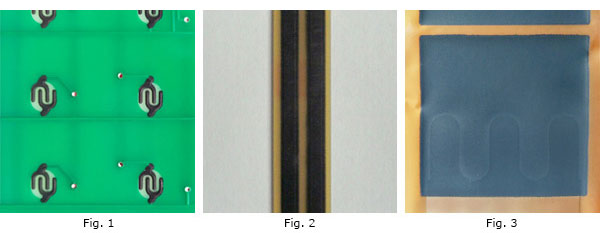
Carbon-printing can be used for several applications. Due to its mechanical strength, the smooth surface and the electrical conductivity it is often used instead of gold for mechanical contacts such as on keyboards (Fic.1) or grinding contacts (Fig.2).
Additional applications are:
- Printed Resistor
- Keyboardfoils for Computers
- Switch contacts
- Blinding
- Heating elements
Thanks to its high flexibility and excellent adhesion, carbon-printing can be printed on polyimid-foils. So it can be used on flexible printed circuit boards too (Fig3).
Carbon-printing is resistant to chemicals, heat, Hot-Air-Leveling and soldering processes. This has the advantage, that the Carbon-contact-areas do not have to be protected before soldering (even wave-soldering) and the value of the resistor will be constant all the time.
Information for the developer:
Carbon-printing has its own resistance which is indicated in Ohm/Square. If the resistance influences the function of the electrical circuit or causes malfunctions, this value must be considered. On a printed square with a coating thickness of 25 microns the resistance can be between 8 and 20 Ohm/Square, depending on the manufacturer. Because of this, the value of the resistance or the manufacturer of the carbon-printing should be specified. The requested resistance value of the circuit can be controlled by an adjustable resistor. Other forms will be specified in Ohm/2Square or Ohm/3Square.
With a resistance measurement you will get the value for Ohm/Square for any square area with a coating thickness of 25 microns. The edge length of the square should be more than 0,315 inch, otherwise the screen printing or the contact resistance of the copper can influence the measurement results.
Please do not hesitate in contacting us for an advice on your next project. We are pleased.
Ask for information on our various possibilities today. Call our specialists or write an e-mail to db@db-electronic.com.
We look forward to your inquiry.
|
|
|
|
Newsletter october 2018
|
Thermal management of metal core PCBs (IMS)
|
|
 |
|
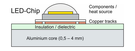
The challenge in high-power applications is to distribute and dissipate the heat (power loss) quickly from components (e.g., LED). The thermal behaviour of an assembly directly affects the life time of the components.
The relevant factors include the dielectric and the soldering processes.
The thermal conductivity of the components is a central matter in the dissipation of heat. While copper and aluminium are excellent at heat dissipating, this does not apply to the dielectric.
The heat starts at the component and dissipates quickly the copper pad. The copper thickness is usually 35 or 70 microns and has a conductivity of about 280 W/mK.
The second layer of the build up structure is the dielectric layer, which restrains the heat due to its poor conductance (usually 60 to 120 microns thick and 0.3 to 3 W/mK specific conductivity).
At an one-sided metal core PCB, the third layer of the build up structure is the metal carrier, which has a good thermal conductance. The thickness of the carrier is usually 1 to 4 mm and its conductivity is 170 W/mK (aluminium) respectively 280 W/mK (copper).
This clearly shows that the main focus is on the insulation layer. The thermal resistance of the dielectric is systemically relevant. It is based on the length and cross section of the heat conduction path and the specific thermal conductivity. Its unit is K/W (Kelvin per Watt).
Usually the thermal potential an aluminium carrier has is not completely exhausted.
The thermal management is not limited to the dielectric. Not only the thermal conductivity should be considered (price sensitive) when choosing a qualified material. Rather more, it is necessary to determine the right dielectric by taking into account the power loss, the usable area and the required insulation thickness. When you compare the thermal conductivity with the thermal resistance does not always seem easy.
In addition, the quality of the soldering processes primarily determines about the dissipation of heat.
Please do not hesitate in contacting us for an advice on your next project. We are pleased.
Ask for information on our various possibilities today. Call our specialists or write an e-mail to db@db-electronic.com.
We look forward to your inquiry.
|
|
|
Newsletter november 2017
|
Press-Fit Technology
|
|
 |
|
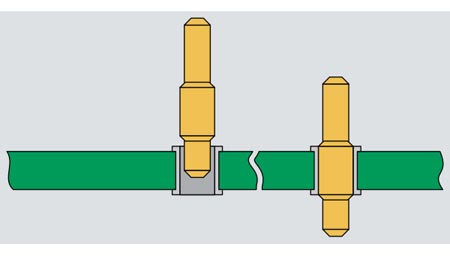
What is it about? Press-Fit is a process in which the components are pressed into plated through holes (PTH) of circuit boards without having them to be soldered.
This process is gaining in importance in various industry sectors, for instance in the automotive industry. The Press-Fit Technology is an advantageous alternative to the assembly of printed circuit boards by soldering.
In order to save space and assembly time, but also in the interest of a higher reliability, more and more wiring harnesses are replaced by printed circuit boards. Pressing in the components is the ideal solution here.
The three most important aspects in this context are:
- Space saving: Integration into the housing
- Increased electrical power: Higher copper thickness and width of the tracks
- Thermal and mechanical resistance: PCBs for high stress applications
The surface finishing is important in this process, using primarily chemical tin (chemical Sn.).
Within your data a clear distinction has to be made between standard drillings with final diameters and press-fit holes, of which the diameter depends on the respective components and is not always easy to determine. Based on your information, we can thus determine the diameter of the finished PTH.
Ask for information on our various possibilities today. Call our specialists or write an e-mail to db@db-electronic.com.
We look forward to your inquiry.
|
|
|
|
Newsletter september 2017
|
High Current Printed Circuit Boards
|
|
|
Printed Circuit Boards for high currents can be etched up to 400 µm copper. In special cases for very high currents, copper substrates with a thickness of 500 to 600 µm are also embedded into a multilayer printed circuit board.
In this context it is particularly important to get in touch with us, as your PCB manufacturer, before designing the layout, to speak about technological specifications and clarify important details.
Press-in contacts are used to ensure a high current for power components and the power supply connection. For applications where the focus is on the heat dissipation, the copper substrate is usually bonded on the surface.
We will gladly advise you on your next project. Call our specialists or write an e-mail to db@db-electronic.com.
We look forward to your inquiry.
|
|
|
Newsletter may 2017
|
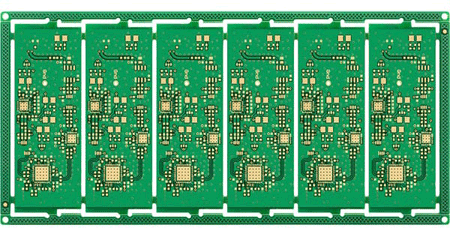
Printed Circuit Boards – single PCB versus panel array?
|
|
 |
|
There is always the question of whether your printed circuit boards should be supplied as a single board or in a panel array. The multiple printed panel often offers the advantage of a more efficient handling during the assembling. This decision has to be made before the layout process. The size and the thickness are as relevant as the frame and the accuracy of the outline.
At db electronic we can machine the PCB panel arrays by milling, V-scoring, step routing with and without perforation, stitch milling eg for round printed circuit boards or laser cutting for flexible polyimide boards.
Thanks to these possibilities we are able to produce the most complicated contours in a panel array.
It is appropriate to contact us in time for a personal consultation, as an optimal utilisation of the production panel has also a positive effect on the price.
We will gladly advise you on your next project. Call our specialists or write an e-mail to db@db-electronic.com.
We look forward to your inquiry.
|
|
|
|
Newsletter january 2017
|
Surface finish for wire bonding
|
|
 |
|
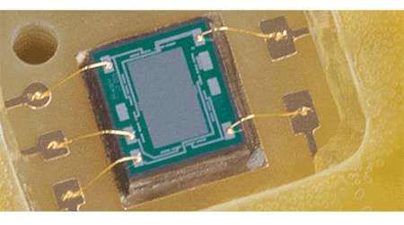
In case of wire bonding, components (eg sensors) are provided with electrical connections using finest wires. The advantage of this process is the short wiring distance, which results in a reduction of the space requirement.
As a PCB manufacturer we need to know if you prefer gold or aluminium wire. That depends on which surface we will apply for a perfect bonding process during PCB production.
While a surface finish with chemical Nickel-Gold (ENIG with a gold thickness of min. 0.07 µm) is sufficient for aluminium wire bonding, Palladium-Gold (ENEPIG) is required for gold wire bonding.
The following paragraphs show the build-up structure of ENIG and ENEPIG:
Layer thickness for aluminium wire bonding
Gold (Au) min. 0,07 µm
Nickel (Ni) 3 - 5 µm
Layer thickness for gold wire bonding
Gold (Au) min. 0,13 µm
Palladium (Pd) min. 0,11 µm
Nickel (Ni) min. 5 µm
We will gladly advise you on your next project. Call our specialists or write an e-mail to db@db-electronic.com.
We look forward to your inquiry.
|
|
|
Newsletter october 2016
|
EPIG – a versatile surface for printed circuit boards
|
|
 |
|
EPIG (electroless palladium / immersion gold) is a nickel-free surface finish. Chemical Palladium Gold is used for multiple applications and the finish is suitable for any kind of solder or bonding applications, for instance Aluminium-wire (Ultrasonic), Gold-wire (Thermosonic) and alternative materials. The palladium layer acts as a diffusion barrier and the gold thickness can be plated up to 0.3 µm due to the semi-autocatalytic nature of the plating bath.
In addition, the surface is suitable for high-frequency applications (no skin-effect) and medical technology (nickel incompatibilities are excluded).
Applications
Reflow soldering and bonding (Aluminium- and Gold-wire), fine line, high-frequency and medical technology
Deposit Properties
Planar finish, nickel-free, solder and bondable (alternative bonding wires), storage time = 12 months, if stored properly
Plating Thickness: 0,1 – 0,2µm Pd/ 0.1 – 0.2 µm Au
Panel Size: from 100 x 100 mm
Panel thickness: from 2 5µm
Aspect ratio PTH: 1 : 16
Aspect ratio BV: 1 : 1 (after copper plating)
We will gladly advise you on your next project. Call our specialists or write an e-mail to db@db-electronic.com.
We look forward to your inquiry.
|
|
|
|
Newsletter may 2016
|
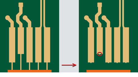
Hole Plugging and Hole Plugged Lands – the alternatives to solder resist covered vias
|
|
|
After we discussed the disadvantages of covering the vias with solder resist in our last newsletter, we would like to present the possible alternatives to you today: Hole Plugging (HP) and Hole Plugged Lands (HPL).
What are behind these terms? Hole Plugging is the filling of vias with a non-conductive paste. This paste fills the vias completely and when used
correctly - without air pockets. Therefore no form of residue will be found in the vias.
|
|
|
The difference between HP and HPL is that the vias in the HPL method are plated-over. Hence, the surface is planar and solderable. HPL is particularly suitable for thermal vias and vias in pad solutions.
We will gladly advise you on your next project. Call our specialists or write an e-mail to db@db-electronic.com.
We look forward to your inquiry.
|
|
|
Newsletter january 2016
|
Covering vias with solder resist – or not?
|
|
 |
|
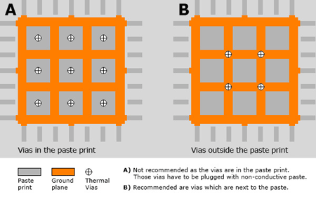
This question arises with increasing frequency due to the increase of even smaller components such as QFP and QFN. Often layouts are designed with solder resist covering from the back, over the vias, to prevent the run off of the paste from the ground planes across to the vias (see fig. A).
Covering of vias involves the risk of chemical residues which affect the further production processes as they cannot be washed out of vias properly. Undefined conditions in the vias and up to the pads take effect in the long-term reliability of the printed circuit board. Therefore covering of vias is not recommended.
The above-mentioned problems can be circumvented with optimized placement of vias and paste print (see fig. B).
If there are no other options, to design the layout according to example A then the vias have to be plugged to ensure a reliably closing of the vias.
See Sealing of drill holes.
We will gladly advise you on your next project. Call our specialists or write an e-mail to db@db-electronic.uk.
We look forward to your inquiry.
|
|

|
|
Newsletter august 2015
|
CTI (Comparative Tracking Index) und PTI (Proof Tracking Index) of base material
The increased packing density of components on the printed circuit boards leads to increasingly smaller conductor track spacings. Therefore, the CTI / PTI value in the base material data sheets gets more important. This is the index for tracking resistance.
Continue to the professional article...
Ask for information on our various possibilities today. Call us or write an e-mail todb@db-electronic.com.
We look forward to your inquiry.
|
|
|
Newsletter march 2015
|
Halogen-free Printed Circuit Boards
In halogen-free printed circuit boards a bromine-free flame retardant is used. Circuits with standard base material and brominated flame retardants can release highly toxic dioxins and furans in case of a fire.
Therefore, halogen-free printed circuit boards in the lighting sector are very popular. The ecological advantage also means a technological lead, focused on a low-emission and future-oriented final product.
In our company, we produce halogen-free FR4 and aluminum printed circuit boards. FR4 printed circuit boards in a thickness of 1 and 1.5 mm, we can produce within one working day. Other designs, we can offer on request. Please ask for specific data sheets.
Learn today more about our technical possibilities. Call our specialists or write an e-mail to db@db-electronic.uk.
We look forward to your inquiry.
|
|
|
|
Newsletter january 2015

 |
|
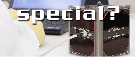
Specialties of db electronic Ltd
When you have a requirement or an idea for an unusual circuit board, and are looking for the right production partner, then you are at the right db electronic. We can advise you on any questions that you might have, regarding design, materials and manufacturing, so that your development is a success.
For example, in 2013 wed had a scientific and technological cooperation with the University of Würzburg, for special aluminum core printed circuit boards, which were used as the housing for a mini-satellites. This satellite has successfully orbited the earth for a year, at a height of 600 kms and is very exposed to large temperature fluctuations daily. Further information.
Therefore, production parameters should already be discussed with your PCB manufacturer in the design phase.
Are you also looking for practical solutions in the field of printed circuit boards? Get together with us for your next project.
Call our specialists or write an e-mail to db@db-electronic.uk.
We look forward to your inquiry.
|
|
|
Newsletter november 2014
|
Impedance on PCBs
Impedance is the technical term for the AC resistance. It will affect the signal transmission on the circuit board. In order to avoid reflections on the printed tracks, which can lead to signal distortions, the impedance of the signal line must be adjusted.
An impedance analysis is always required when fast switching signals at low current to be transmitted, as these are most susceptible to interference.
Therefore, production parameters should already be discussed with your PCB manufacturer in the design phase.
We offer
• the manufacturing of Impedance tested PCBs
• the simulation of impedances and if necessary modifications before
production start-up
• a measurement protocol by means of a TDR device
For further information please visit also
www.db-electronic.com/en/pcb-manufacturing_s55.htm.
Call our specialists or write an e-mail to db@db-electronic.com.
We look forward to your inquiry.
|
|
|
|
Newsletter september 2014
|
New at db-electronic.com: ODB++
ODB++ is a proprietary data format for the efficient data exchange between all involved departments of the development of electronic systems. It can contain all the data for production, from the schematic (CAD) to the production data of the PCB (CAM), but also the mounting and housing configuration.
With ODB++ files all relevant information are available, including layer construction, drilling and milling programs and fiducials, no additional documents are required. We process all standard formats and digitize existing templates.
No matter which data format you prefer, we can implement it!
Take this opportunity and inform yourself right away about our advantageous deals at www.db-electronic.com/en/pcb-production_s01.htm.
Call our specialists or write an e-mail to db@db-electronic.com.
We look forward to your inquiry.
|
|
|
Newsletter july 2014
|
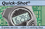
Not just when it’s urgent!
As a long time manufacturer of PCBs, we offer tailor-made packages for your board needs, depending on your lead times or other factors that are important to you. |
|
 |
|
|
Quick-Shot
With Quick-Shot you benefit from the ultimate in express service. Deliveries normally within only 3 days, but on request, can sometimes be faster. You can be assured that we will deliver your order on time, to your specification and to your complete satisfaction.
Check also www.db-electronic.com/en\pcb-production_s01.htm on our new website. For more information about our wide range of products and services pleae call or send us an e-mail to db@db-electronic.com.
We look forward to your inquiry.
|
|
|
|
Newsletter
|
Subscribe here for our newsletter!
|
|