 |
|
||||
|
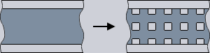
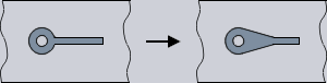
01 | 02 | 03 | 04 | 05 | 06 | 07 | 08 | 09 | 10 | 11 | 12 | 13 | 14 | 15 | 16 | 17 | 18 | 19 | 20 | 21 | 22 | 23 | 24 | 25 | 26 | 27 | 28 | 08 – Rigid-flex PCBsDesign guidelinesThe following design guidelines should help to avoid the most frequent errors when developing a rigid-flex PCB.• Make sure that the structure is symmetrical. • Avoid an all-over copper surface in the flex area. • The throughplating should be located in the rigid area, with a sufficient distance from the rigid-flex transition. • Avoid a change in direction of tracks in the flex area, or keep it to a minimum. • Thicker "blind tracks" above and below as tear protection. • Drill holes in the rigid area should be set back from the edge (at least 2–3 mm). • Do not route tracks parallel to the bend radius as there is a risk of fracture. The best solution: route tracks in straight lines on the flex layer. • The entire surface of the flex layer can be used for routing in the rigid area. Performance specifications can be found under IPC standard 6010 (6013 for flex PCBs) and IPC 2223 for the design. Examples
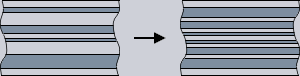
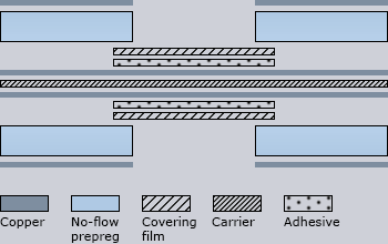
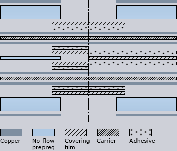
08.1 Standard structure of rigid-flex PCBsBelow you will find some schematic drawings of standard stack ups. This is just a small selection of possible rigid-flex connections.Rigid-flex PCBs with flex in the inner layerIn version 1, the standard structure illustrated by a 2-sided flex carrier in the inner layer.In version 2a, a prepreg is inserted between the two flex layers in the rigid area. The benefits of this version are the greater flexibility and the opportunity of assembling the layers independent of each other. In version 2b, both flex layers are glued to each other. The rigid-flex connection thus becomes less mobile but is cheaper. Disadvantage: On warming the adhesive promotes the expansion of the Z-axis.
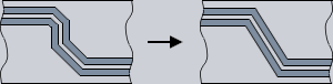
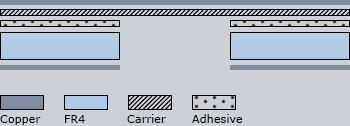
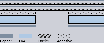
Rigid-flex PCBs with flex on the outer layerEasier to create are flex connections on the outer layer, as FR4 is used, clad in copper foil on one or both sides. The flex layer is press-moulded to the base material using an adhesive.
Technical Data
Semiflex – the alternative for one-off installationSemiflex is a very thin FR4 material, which is particularly suitable for one-off installations and cases where it will not be dynamicly stressed.Feasible designs • Copper: 18 / 35 µm • FR4: 125 µm • max. area: 250 x 400 mm |