|
|
|
previous page |
overall view |
next page
01 |
02 |
03 |
04 |
05 |
06 |
07 |
08 |
09 |
10 |
11 |
12 |
13 |
14 |
15 |
16 |
17 |
18 |
19 |
20 |
21 |
22 |
23 |
24 |
25 |
26 |
27 |
28 |
12 – Solder resist varnish on printed circuit boards
The purpose of solder resist varnish is to protect the copper tracks from oxidation and to prevent solder bridges in case of wave soldering or reflow soldering. The type of solder resist varnish must be selected according to the fineness of the pattern layout and the structural elements being assembled.
In case of conventional assembly using axial and radial components, if a thermal 2-component or UV-hardened mask applied using screen printing is possible, then the use of photostructurable solder resist masks (photosensitive, photoimageable solder masks) are preferred in the case of SMD structural elements. All masks meet the IPC-SM-840 Class III standard.
Typical standard layer thicknesses over the conductor are 7 – 10 μm, and over the edge of the conductor at least 3 – 5 μm. On customer's request, however, other layer thicknesses are possible. Structures of 150 μm can easily be covered.
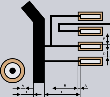
Note: If you are using fiducial marks or registrations on your PCB, then we recommend providing generous cutouts for these in the solder resist mask. Place the pad rows just sufficiently distant to each other to leave a solder resist tab of 200 μm.
 |
|
| |
screen printing
mask |
photosensitive
solder resist
varnish |
| A Cutout in mask |
0,25 mm |
0,08 mm |
| B Distance mask / conductor |
0,15 mm |
0,075 mm |
| C Distance copper / copper |
0,4 mm |
0,15 mm |
| D Minimum tab width |
0,5 mm |
0,1 mm |
E Distance Pad / Pad
|
1,0 mm |
0,25 mm |
|
|
|
|
|
|