|
|
|
previous page |
overall view |
next page
01 |
02 |
03 |
04 |
05 |
06 |
07 |
08 |
09 |
10 |
11 |
12 |
13 |
14 |
15 |
16 |
17 |
18 |
19 |
20 |
21 |
22 |
23 |
24 |
25 |
26 |
27 |
28 |
18 – PCB pattern layout – structure and width of tracks
Structure
The pattern layout will be structured according to the procurement documentation and will generally look as follows:
1. Copper base
2. Chemical copper / conductive graphite layer
3. Electrolytic copper up to the required final dimensions
4. Surface protection through hot-air levelling, solder resist
varnish, etc.
Individual components of the circuit pattern, e.g. a track, can become broader or narrower due to errors in exposure, too strong or weak etching, or through galvanising errors. This results in an edge offset either inwards or outwards. The nominal values of the pattern layout are specified through the CAD data provided and through the films inspected by the PCB supplier respectively. |
|
For the measurements, the vertical projection P of the pattern layout on the PCB applies.
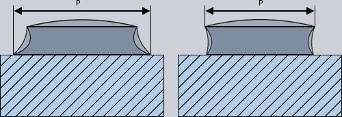 |
Width of printed tracks
For the width of the printed tracks (CAD data or film), the maximum permitted tolerances according to DIN IEC 326 T3, Class "very fine": +0,03/-0,05 mm. In spite of the vertical projection, these tolerances shall also apply for the entire track cross-section, so that possible under-etching in the case of the minimal track width must be taken into account.
The admissibility of individual faults that may occur, such as notches, pores and holes, is specified in the figure on the right. On average, no more than 1 fault may occur per 50 mm of track length.
If the length of a fault exceeds the 3 mm, then a repair can be done.
|
|
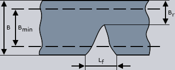
B Width of track (nominal value)  5 mm 5 mm
Bmin minimum track width (nominal value minus tolerance)
Br Residual track width ≧ 0,8 Bmin
Lf Length of the fault 3 mm |
18.1 – Insulation spacing and soldering pads
Insulation spacing
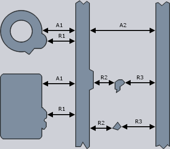
The pattern spacing R between the individual parts of the pattern layout of the outer and inner layers (tracks, pads, etc.) is provided by the width tolerances of the pattern layout stated above.
Unwanted metallic particles that are present by chance, and tracks projections must be taken into account in judging the insulation spacing and may not reduce the nominal insulation spacing A by more than 50 μm. |
|
|
 |
|
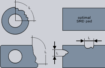
Soldering surfaces
The width of the annular ring of a land or the width and length of a SMD soldering pad must not be reduced to below 75% of its nominal value due to local faults (such as notches on the edge).
The following additional restrictions apply for the length of the notch:
• Land for hole assembly: Length L = 90° or 25% of the perimeter
• SMT soldering pads: Length L = 25% of the edge length of the perimeter
• The nominal surface of the land and soldering pads may be reduced by a maximum
of 10% through faults and irregularities. |
18.2 – Defects in metallized holes
The metallization of through platings must have a sealed surface. There must be no defects at the transition between the barrel/pad or at the contact point of the inner layers.
The transition area is the area that extends from the PCB surface into the hole to 1,5 times the total thickness of the copper layer available or, in case of inner layers, twice the thickness of the copper layer of the inner conductor level.
Faults at diametrically-opposed points in the hole wall are not permitted, as these indicate a circumferential tear. |
|
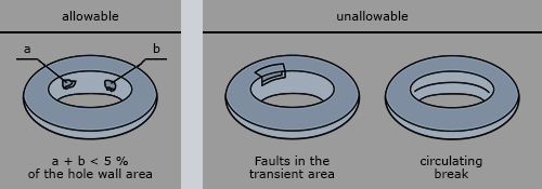
Certain faults are permitted under the following conditions:
• Not more than 3 faults may occur in a maximum of 0,5% of the metallized drill
holes.
• The total area of the faults in one drill hole may not exceed 5% of the total
wall surface of the drill hole.
• The biggest dimension of such faults must not exceed 25% of the
circumference in a horizontal direction and 25% of the board thickness in a
vertical direction. |
|
|