 |
|
||||
|
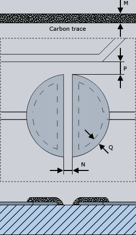
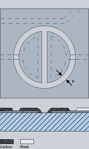
01 | 02 | 03 | 04 | 05 | 06 | 07 | 08 | 09 | 10 | 11 | 12 | 13 | 14 | 15 | 16 | 17 | 18 | 19 | 20 | 21 | 22 | 23 | 24 | 25 | 26 | 27 | 28 | 19 – Carbon paste printing in the PCB productionApplicationCarbon paste is applied using screen printing as a keyboard contact or LCD contacts and strips. Preconditions The requirements listed in the following presuppose a thickness of 17,5 μm of the copper foil on the laminate. Materials A fine- or coarse-grain conductive carbon paste will be printed. Degree of detailing of the pattern layout when screen printing with carbon paste As the printing accuracy of carbon paste depends on the grain size, the PCB manufacturer must select the carbon paste type according to the degree of detailing in the sample conductor unless the customer has specified a particular paste. The degree of detailing is determined by the parameters listed below. The values that are decisive for the design are listed separately for photopolymer masks and carbon screen printing. M Printing width of the pattern layout – photopolymer 0,3 mm / screen printing 0,5 mm N Insulation spacing carbon/carbon – photopolymer 0,3 mm / screen printing 0,5 mm P Insulation spacing carbon/copper – photopolymer 0,5 mm / screen printing 0,7 mm Q Overlap carbon/copper – photopolymer 0,3 mm / screen printing 0,5 mm R Spacing carbon/solder resist mask – photopolymer 0,3 mm / screen printing 0,5 mm
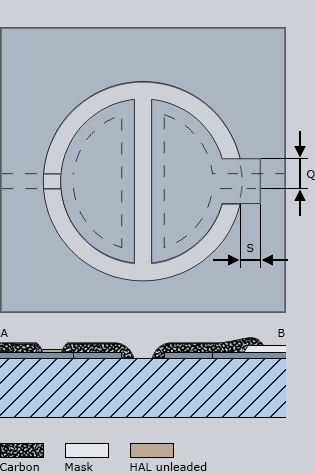
19.1 – Overlap in carbon paste printingThere should be no exposed tracks that could connect carbon elements if the following conditions are met (fig. 3):Q Overlap carbon/copper – photopolymer 0,3 mm / screen printing 0,5 mm S Overlap carbon/solder resist mask – photopolymer 0,4 mm / screen printing 0,5 mm Design information: Version A (fig. 3, on the left) includes the hot-air levelling technique to protect the copper surface. In this case, the carbon layer must not be protected by a strippable mask. Version B (fig. 3, on the right) has a copper circuit, where the carbon print covers the mask to a certain extent and thus protects the connection point of the conductor. |