|
|
|
previous page |
overall view |
next page
01 |
02 |
03 |
04 |
05 |
06 |
07 |
08 |
09 |
10 |
11 |
12 |
13 |
14 |
15 |
16 |
17 |
18 |
19 |
20 |
21 |
22 |
23 |
24 |
25 |
26 |
27 |
28 |
06 – Standard construction of multilayers
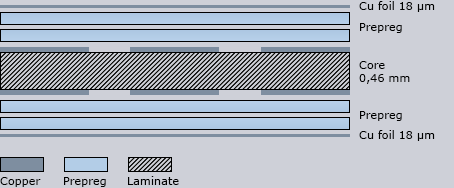
06.1 Standard stack up for 4-layer multilayers (1,0 mm nominal thickness)
Unless otherwise stated in the order, we will use the following stack up for all 4-layer multilayers with 1,0 mm nominal thickness.
The nominal thickness of the press-moulded layer package without galvanic structure is 1,0 ± 0,11 mm. The layer structure of the multilayer consists of a 0,46 mm thick base material core, foil-clad with 35 μm of copper on both sides, 2 prepreg layers and a 18 μm thick copper foil as a basis for the exterior layers.
In order to keep twist and warp within the permitted tolerance, the multilayer must be constructed symmetrically.
|
|
 |
06.2 Standard stack up for 4-layer multilayers (1,6 mm nominal thickness)
 |
|
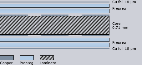
Unless otherwise stated in the order, we will use the following stack up for all 4-layer multilayers with 1,6 mm nominal thickness.
The nominal thickness of the press-moulded layer package without galvanic structure is 1,60 ± 0,20 mm. The layer structure of the multilayer consists of a 0,71 mm thick base material core, foil-clad with 35 μm of copper on both sides, 2 prepreg layers and a 18 μm thick copper foil as a basis for the exterior layers.
In order to keep twist and warp within the permitted tolerance, the multilayer must be constructed symmetrically.
|
06.3 Standard stack up for 6-layer multilayers (1,6 mm nominal thickness)
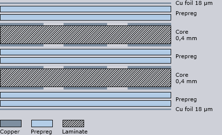
Unless otherwise stated in the order, we will use the following stack up for all 6-layer multilayers with 1,6 mm nominal thickness.
The nominal thickness of the press-moulded layer package without galvanic structure is 1,6 ± 0,2 mm. The layer structure of the multilayer consists of two 0,40 mm thick laminates, foil-clad with 35 μm copper on both sides, separated from each other through 2 prepreg layers (2116) and by an 18 μm thick copper foil as the basis for the exterior layers.
In order to keep twist and warp within the permitted tolerance, the multilayer must be constructed symmetrically.
|
|
|
06.4 Standard stack up for 8-layer multilayers (1,6 mm nominal thickness)
|
|
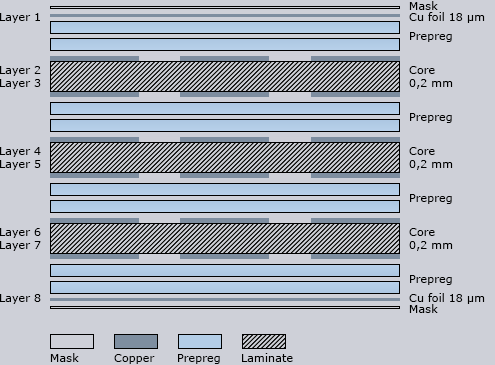
Unless otherwise stated in the order, we will use the following stack up for all 8-layer multilayers with 1,6 mm nominal thickness.
The nominal thickness of the press-moulded layer package without galvanic structure is 1,6 ± 0,2 mm. The layer structure of the multilayer consists of three 0,20 mm thick laminates, foil-clad with 35 μm of copper on both sides, separated by 2 prepreg layers (2116) and separated from each of the exterior layers with a single layer (2116) + ( 1080 ) of prepreg.
In order to keep twist and warp within the permitted tolerance, the multilayer must be constructed symmetrically.
|
|
|