 |
|
||||
|
01 | 02 | 03 | 04 | 05 | 06 | 07 | 08 | 09 | 10 | 11 | 12 | 13 | 14 | 15 | 16 | 17 | 18 | 19 | 20 | 21 | 22 | 23 | 24 | 25 | 26 | 27 | 28 | 26 – Design rules for FR4 semi-flex PCBs
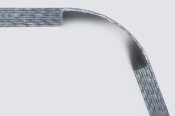
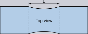
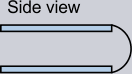
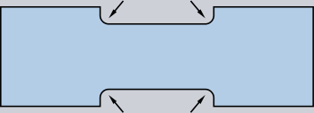
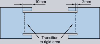
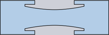
26.1 – Parameters for semi-flex PCBs with 1 copper layerThe length of the semi-flexible area depends on the bending radius required:• Bending radius 90 degrees – L ≧ 10 mm • Bending radius 180 degrees – L ≧ 20 mm Bending for semi-flex PCBs is only allowed at the depth-milled section (copper on the outside). Example 1: Semi-flexible area is as width as the PCB
Example 2: Transition from semi-flexible to rigid areas
Example 3: Bending area inside the PCB
Relevant information• Semi-flex PCBs are not designed for multiple bends, but for one-time bending (flex-to-install).• The semi-flexible area must be bend very carefully. A controlled pre-bending by using a bending tool is recommended. • The ridig parts of the PCB must be screwed to the housing or a carrier to relieve the bending area. • The semi-flexible area has usually a thickness of approx. 0.25 mm. • The longer the semi-flexible area L, the less it will be stressed. • The copper layers must always be on the outside – see below. 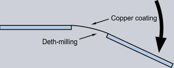 |