 |
|
||||
|
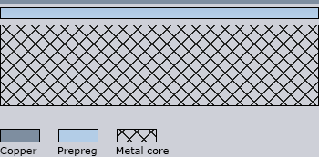
01 | 02 | 03 | 04 | 05 | 06 | 07 | 08 | 09 | 10 | 11 | 12 | 13 | 14 | 15 | 16 | 17 | 18 | 19 | 20 | 21 | 22 | 23 | 24 | 25 | 26 | 27 | 28 | 09 – Heatsink PCBsHeatsink PCBs are understood as PCBs that are able to dissipate high surface temperatures. Generally, these temperatures are caused by power semiconductors (transistors, thyristors, diodes and LEDs) as well as resistors. The following methods are suitable to dissipate the heat:• The use of heat transfer compounds • Higher copper thicknesses • Heat dissipation using a metal core • Heat dissipation using a metal heat-conducting plate 09.1 – Heat transfer compound (single-component paste)The heat transfer compound is applied in a similar way to the silkscreen using a screen-printing procedure. The thickness of this layer is approx. 100 – 150 μm.09.2 – Higher copper thicknessesIn case of thick-copper boards, the heat is absorbed and dissipated directly by the copper. Here, the copper thicknesses are at least 105 μm, 210 μm or 400 μm. The disadvantage of this technology, however, is that fine conductor structures can only be achieved with much effort and therefore the production is thus costly.09.3 – Heat dissipation using a metal core
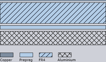
09.4 – Heat dissipation using a metal heat-conducting plate
Possible solutions• PCBs made from metal core material• Alternatively, self-press-moulded base material • Double-sided through-plated PCBs (aluminium-core PCBs) • Standard production, single-sided PCBs with subsequent press-moulding with aluminium • PCBs with heat-transfer compound Technical informationMetal core PCBsFinished laminated aluminium base material from various manufacturers, with special prepregs (thermal conductivity from 1 W/mK) Alternative design Self press-moulded aluminum base material with "no-flow"-prepreg 0,1 mm and copper foil in various thicknesses Single-sided PCBs using standard technology FR4 carrier with single-sided copper is press-moulded to the aluminium using prepreg 0,2 mm. The thickness of the aluminium is approximately 1,2 – 1,6 mm Heat-transfer compound Single-component heat sink paste, HSP 2741, black, made by the Peters company, using screen-printing procedure Thick copper PCBs Only possible to 210 μm. At this thickness, problems may occur with the solder resist varnish (flank coverage, dependent on layout). In this case, the gaps are filled with paste. Min. width and gaps of tracks: 1,0 mm |