 |
|
||||
|
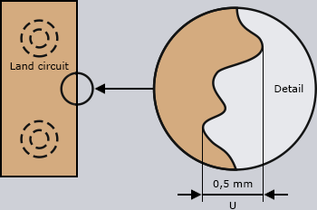
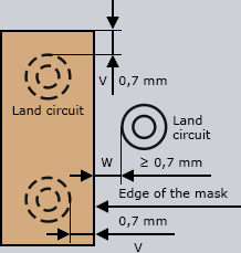
01 | 02 | 03 | 04 | 05 | 06 | 07 | 08 | 09 | 10 | 11 | 12 | 13 | 14 | 15 | 16 | 17 | 18 | 19 | 20 | 21 | 22 | 23 | 24 | 25 | 26 | 27 | 28 | 15 – PCB manufacturing – Peelable masksApplicationPeelable masks are used to cover particular drill holes of a PCB, so that no solder penetrates during machine soldering. They also protect carbon elements and gold contacts during this process. Peelable masks are applied by screen printing.Requirements• The peelable mask must adhere sufficiently well to the PCB so that it does not peel off when handled correctly.• It must be able to endure a two to three time soldering process without peeling off, but must remain detachable. • After soldering of the PCB, the peelable mask must be able to be detached – preferably in one piece. In case of metallized holes, no mask residue must be left in the drill holes or on the surface of the PCB. In the case of non-metallized drill holes, however a certain amount of residue can remain. • The peelable mask must be able to resist conventional solvents such as chlorinated and fluorinated hydrocarbons, isopropanol, conventional fluxes and similar. • Particular requirements: The roughness U of the edge of the mask can be 0,5 mm from the tip to the base (left figure below).
|