|
|
|
previous page | overall view | next page
01 | 02 | 03 | 04 | 05 | 06 | 07 | 08 | 09 | 10 | 11 | 12 | 13 | 14 | 15 | 16 | 17 | 18 | 19 | 20 | 21 | 22 | 23 | 24 | 25 | 26 | 27 | 28 |
28 – Connections for gold plugs (galvanic gold plug plating)
Galvanic gold is always used when contacts are mechanically loaded. These can be plug contacts (e. g. computer plug-in cards) or grinding rings for switching contacts. Galvanic gold is more resistant to abrasion, as the layer thickness and hardness are higher than with chemical gold. The chemical gold serves as a protective layer for the nickel layer underneath and has only a thickness of about 0,05 μm. Galvanic gold has a minimum layer thickness of 0,8 μm.
In order to galvanize plugs or pads, a so-called help line is required, which connects the contacts electrically to the outside. Alternatively, the corresponding contacts can be gold-plated even before the etching process. In this case, no help lines are needed, as the production panel still has a full-surface copper coating. The gold-plated surfaces later also serve as an etching resistance. Disadvantage: this process is more complex and is only used in special cases. In addition, gold-plated contacts may be underetched.
 |
 |
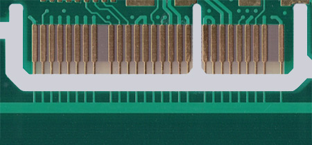
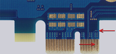
Fig. 1 – Gold connector
Here the contact line has not yet been chamfered. The help lines as well as the current collector rail underneath are clearly visible.
|
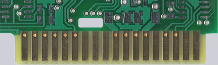
Fig. 2 and 3 – Gold connectors chamfered
With chamfered plug contacts, the help lines are removed almost up to the contacts, depending on the bevel angle and clearance of the bevel.
A special problem is the connection of shorter contacts. They must not be connected downwards with help lines, as they should not make contact until later when plugged in. |
|
|
|
|
There are 3 possibilities to connect shorter contacts:
1. The contacts are led out of the PCB via additional tracks at another point and then separated during outline processing (Fig. 4 and 5).
2. The help lines are mechanically removed with a Z-axis milling. The problem here is that copper burrs and edges can arise.
3. An additional intermediate step removes the help lines at the etching process.
|
 |
|
|
|
If possible, version 1 should be chosen as it does not require any extra effort. However, corresponding tracks have to be taken into account in the layout.
If it is not possible to direct the contact connections to the outside, the third method is used. Although it is more complex and therefore more expensive, it ensures a clean conclusion of the contacts.
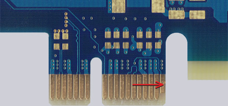
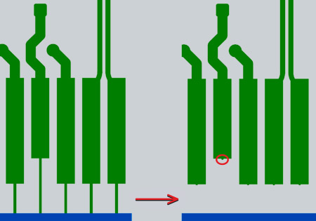
Fig. 6 (right)
Contacts before and after removing the help lines |
|
 |
|
|