 |
|
||||
|
01 | 02 | 03 | 04 | 05 | 06 | 07 | 08 | 09 | 10 | 11 | 12 | 13 | 14 | 15 | 16 | 17 | 18 | 19 | 20 | 21 | 22 | 23 | 24 | 25 | 26 | 27 | 28 | 24 – Impedance on PCBsWhy to consider the impedance?An impedance analysis is always required when fast switching signals at low current to be transmitted, as these are most susceptible to interference. Impedance is the technical term for the AC resistance Z0.It will affect the signal transmission on the circuit board. In order to avoid reflections on the printed tracks, which can lead to signal distortions, the impedance of the signal line must be adjusted. There are two types of impedance:
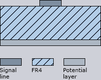
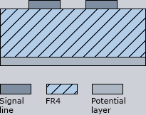
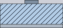
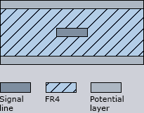
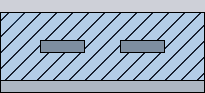
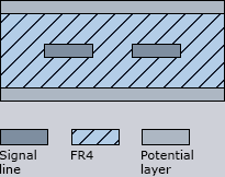
Both impedance types may occur in various combinations, such as on an outer layer or in an inner layer. Signal lines with only one potential layer are called «microstrip», signal lines between two potential layers «stripline». Beispiele
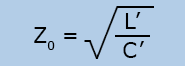
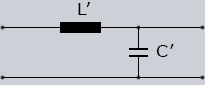
Basically, the signal line of a circuit board is a combination of resistance R, inductance L and capacity C. The inductance is dependent on the conductor width and conductor spacing, while the capacity is dependent of the distance between conductor and potential layer.
The impedance is thus dependent on • the trace width (single-ended) or trace width and trace spacing (differential pairs) and thickness • the thickness of the dielectric (prepreg = distance to the potential layer) • the dielectric constant of the dielectric For the production of Impedance tested PCBs the following information is required: • Number of layers • Layer structure (layer distances / prepregs and cores as well as the copper thickness of the individual layers) • PCB thickness • for the impedance analysis: • which type of impedance (single ended or differential pairs) and value (eg. 50 or 100 ohms)? • what layers are relevant and what are the associated potential layers (reference layers)? • what tracks are relevant (trace width and spacing)? |